Identify and unlock the full potential of your manufacturing operations.
Welcome to the cutting-edge of semiconductor innovation, where Multi-Project Wafer (MPW) solutions are transforming the landscape of chip development. At the forefront of this revolution stands MapSuite, empowering engineers and innovators to harness the full potential of MPW technology.
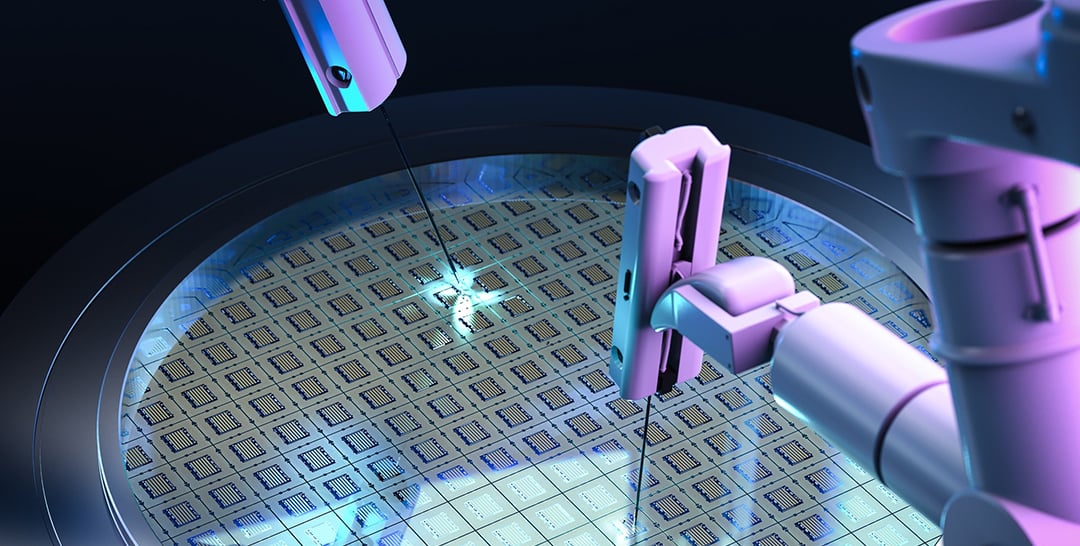
A Multi-Project Wafer (MPW) service enables multiple designs from different creates, to be fabricated together on a single semiconductor wafer. This shared fabrication process allows for cost-effective prototyping and low-volume production, making MPW solutions ideal for startups, research projects, and small-scale semiconductor development efforts.
MapSuite offers a comprehensive suite of tools and resources tailored to streamline the MPW process, providing engineers with the flexibility and efficiency needed to bring their designs to life.
Embark on a journey of innovation with MapSuite’s MPW solutions. Explore the possibilities of semiconductor development with cost-effective MPW fabrication, backed by MapSuite’s industry-leading tools and support. Whether you’re a startup, research institution, or established semiconductor firm, MapSuite empowers you to realize your vision and drive technological advancement.
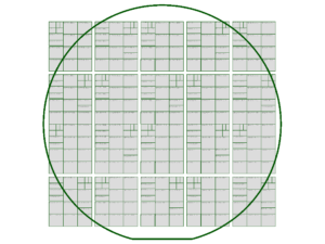
MPW Visualization: MapSuite simplifies the integration of diverse designs onto a single visualized wafer, allowing engineers to view and analyze chip layout and maximize wafer utilization. With MapSuite’s intuitive interface, designers can seamlessly see their results projects with ease.
Collaboration and Compatibility: MapSuite fosters collaboration among different project stakeholders, facilitating seamless communication and coordination throughout the MPW process. Compatible with a wide range of design formats and fabrication technologies, MapSuite ensures compatibility across diverse project requirements.
Design Verification and Simulation: MapSuite provides powerful verification and simulation tools to ensure design integrity and optimize performance. Engineers can visualize and analyze their designs in detail, identifying potential issues and making informed decisions to enhance overall chip quality.
Cost Optimization and Scalability: By leveraging MPW solutions through MapSuite, engineers can significantly reduce fabrication costs and minimize time-to-market. MapSuite’s scalable infrastructure accommodates projects of all sizes, from small-scale prototyping to full-scale production runs.