Identify and unlock the full potential of your manufacturing operations.
Identify and unlock the full potential of your manufacturing operations.
MapSuite provides a modern and comprehensive approach to substrate map management, addressing key challenges including yield optimization, process monitoring and control across all production stages, and multi-site equipment integration. Built on a state-of-the-art architecture and an intuitive, web-enabled user interface, MapSuite delivers targeted functionalities that enhance efficiency and precision.
Despite decades of standardization and automation, substrate map management remains a challenge in high-precision manufacturing, where traceability and process accuracy are critical. Governed by industry standards like SEMI E142, many manufacturers still rely on outdated legacy systems or custom-built solutions. More than just software, MapSuite is a comprehensive solution designed to address these challenges through a modern, fully integrated approach. It supports substrate traceability throughout the wafer lifecycle, enabling die-level data tracking – from initial processing to final testing and assembly.
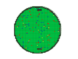
Show visually the substrates in a web-browser, so the user has an overview of how production results look like.

Many different substrates are supported, being it semiconductor or photonic wafers. Also lead- frames and trays are supported, or even single products. As well as waffle and gel packs can be used.

Substrates can be manually edited, when for example additional fail dies are found in a process, or when certain parts of a substrate should not be used for further processing.
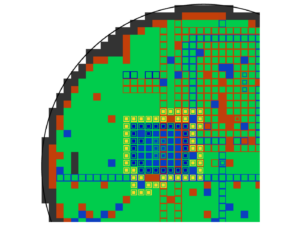
Merge production results of the substrate from different processes, having always updated substrates maps available.
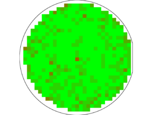
Stack bin results of a substrate map, to find common failures on certain positions of a wafer. For example, to judge which edge dies should have standard the status failed.
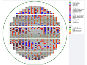
Store visual inspection results and have them available for an overlay with other production results, or merge the result with other substrate data.
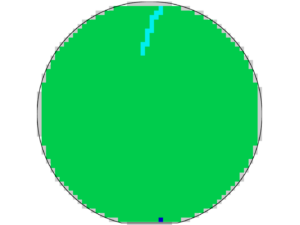
Substrates like wafers are sensitive for chipping and scratches. This gives the need for the option to indicate where wafers are chipped or scratched.
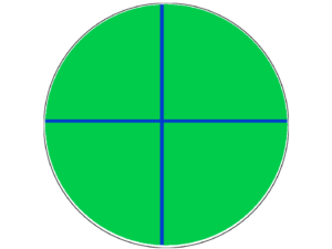
Sometimes wafers can break, but the products on the non-broken part will still work. Or a substrate needs to be split for different processes, like bars in the photonics world.

For high value, medical and automotive devices it is almost a must to have full traceability from the die on the wafer to the individual dies in an end product, a transfer map can help in this process.
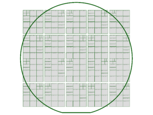
With the increasing price and complexity of products, sample products are many times created using Multi Project Wafers. Those substrates are also supported.
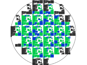
Chiplets as well as a system in a package can be handled with MapSuite. Having different dies in one package next to each other, or stacked, it becomes all possible.
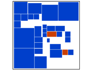
For this process substrate maps can be used for assembly. Like an electronic map for the die attacher, or a coat and cleave plan for the photonics industry.

Particle inspection data, obtained from various sources including microscopes and automated inspection equipment like KLA machines, provides critical insights into substrate defects and particle presence.
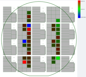
At test and assembly, it is sometimes desired to see a real time map of production, but the equipment is not capable of that, MapSuite can help here out as well.
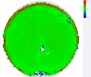
Many times, production runs at different locations, with the Multi Site Option data can be exchanged between different locations within the company. But substrate maps can also be exchanged with subcontractors for example - in both ways, receive and send.

Over the years many file formats to contain the substrate information have been introduced. The base of MapSuite is the E142 map, while supporting 50+ other formats. File conversion is therefore standard available.
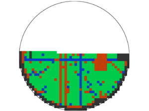
At test and assembly, it is sometimes desired to see a real time map of production, but the equipment is not capable of that, MapSuite can help here out as well.

Often production runs at different locations, with the Multi Site Option data can be exchanged between different locations within the company. But substrate maps can also be exchanged with subcontractors for example - both ways, receive and send.
This is where it all started 20+ years ago, from inkless binning to electronic substrate maps. 1 or 1,000,000 parts on a wafer, MapSuite can do and has done it all.
So far this has been a high-tech low volume market, but we see this growing like semiconductors. It has some additional requirements, MapSuite supports those, like the layout for bars to name one.
Who doesn’t know the flexible PCBs that go into your camera. These days even a cable harness of a car can be made with a flexible substrate. As in production more than one substrate on a larger substrate goes through the factory, having a tool that can support those can become very useful.
Power resistors are made on so called ‘plates’ as being the substrate. A couple of 100 resistors can sit on such a plate, and those need to be singulated in the end and sorted. MapSuite can help to handle those substrates.
The semiconductor way of putting layers on a substrate, layer by layer, is something that is used to make nano-mechanical parts. For example, the small tools that make the gripper that can go into your blood vessels are made in this way. Layer by layer those small parts are created so they can make small mechanical structures that are able to ‘move’.
Laser cutters and Engraving equipment can handle sheets with several parts at the same time. To control the quality of those sheets, MapSuite can be used to store those sheets as substrates, and make use of the solutions available, like editing the sheet to mark bad parts for example.
Select 15 or 30min session for your first appointment and choose a time slot.
Please, let us know your three most important requirements for our preparation of the appointment.